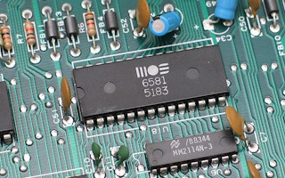
Printed circuit boards (PCBs) are best recycled by pulverising them into nanosized particles to easily recover valuable constituents such as polymers, oxides and metals, say Indian researchers.
The new method, described in a study published in Materials Today in March, is scalable and environment-friendly, said researchers from the Indian Institute of Science (IISc), Bangalore, and the Rice University in Houston, US.
In the study, the researchers followed the principle that ultra-low temperatures make materials brittle and are easy to pulverise and separate.
They placed a PCB in a rotating cylinder with temperatures brought down to minus 119 degrees Celsius before bombarding it with steel balls to shatter it into nanoparticles which were then dispersed in water.
The nanoparticles could be put to various uses, the researchers said. They could be added to polymer composites strengthening them, used in 3D printing or in the making of polymer powder-based paints.
Metallic nanoparticles can be reused after purification by well-known methods.
“With some preliminary sorting, the method can handle most PCBs, says Kamanio Chattopadhyay, research guide, professor at IISc and an author of the study.
Although the technology is still in the laboratory stage, the research team is now working with an industry to demonstrate its scalability and effectiveness.
“
With some preliminary sorting, the method can handle most PCBs.
Kamanio Chattopadhyay, research guide and professor, India Institute of Science
Scaling up the process depends on factors such as the existence of an efficient supply chain of waste as well as viable business models “including the availability of capital, expected return and the policy environment,” says Chattopadhyay.
Others are less optimistic.
“Physical crushing requires a lot of energy, especially when dealing with complex circuit boards with a variety of components.
Smelting circuit boards is more economical and feasible,” says R. Parthasarathi, managing director of E-Parisara, one of India’s leading e-waste recycling companies.
According to the United Nations University, the world produced 42 million tonnes of e-waste in 2014, with Asia accounting for 16 million tonnes.
Currently e-waste is dumped in landfills, incinerated or treated with chemicals to recover valuable materials, but these are not regarded as environment-friendly processes.
This piece was produced by SciDev.Net’s Asia & Pacific desk.